Research in the Laboratory
We are developing the following research themes focusing on advanced research related to solid state chemistry, including the development of teaching materials .
Development And Application of Nanocrystalline Materials Using Nanoscale Electrocrystallization
Functional Manifestation by Inkjet Patterning of Biomaterials and Its Application
Function and Physical Properties of Organic-inorganic Hybrid Perovskite Compounds
Development of Programming Materials Suitable for Science Classes (Faculty of education)
Development And Application of Nanocrystalline Materials Using Nanoscale Electrocrystallization
Toward highly efficient nanofabrication
“How do we put nanomaterials where you want?” This is still awaiting solution in the nanotechnology field. Many trials are now in progress. We cannot pick them up with tweezers because they are invisible. In addition, when we build it up one by one, it takes time and is inefficient. Highly efficient nanofabrication is required for electronics based on nanotechnology.
Then, what is “highly efficient nanofabrication”? First, it should be simple and energy-saving. Recent semiconductor industry requires high temperature and/or high vacuum conditions. We can say that the more energy-saving it is, the more efficient it is. Second, it should be pin-point fabrication. We usually fabricate thin-film-based various devices. However, because we mostly have to remove unnecessary part of the film, the material of the unnecessary part will be a waste. It is efficient that we can fabricate the material only where we want. Finally, nanomaterials should be high performance. When the nanomaterial is high performance, the device based on the nanomaterial becomes highly efficient. Generally, in the case of organic devices, it become high performance when we utilize single crystal.
From the viewpoint, we focused on an electrochemical method which enables us to fabricate organic nanocrystals in a solution, and we are trying to apply the nanocrystals to various devices.
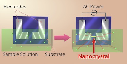
Site-selective fabrication, “nanoscale electrocrystallization”
The “electrocrystallization” is known as one of the method for preparing organic conductors. In this method, electrolysis (electrochemical reaction) gives organic materials charge carriers that are conductive sources, and at the same time organic molecules with a π-electron system gather and are visible mainly on the electrode surface. Form crystals of size. After electrolysis, the electrode can be taken out and crystal can be obtained by scraping off the crystal attached to the electrode.
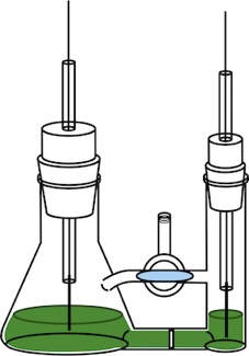
Figure: Electrochemical cell for (bulk) electrocrystallization
In this research theme, “Nanoscale Electrocrystallization” was first presented in 2002 and published in 2003 as a novel method for preparing nanoscale crystalline materials based on the method. In order to produce invisible nano single crystals, two electrodes used for electrolysis were placed on the substrate. If a nanoscale single crystal can be arranged to bridge between two electrodes, the nanoscale single crystal can be utilized as various devices. In other words, after electrolysis, it can be taken out of the solution and then utilized for the device as it is. A simple and energy-saving device fabrication method is realized. From this reason, the two electrodes on the substrate are made so that the tips faced closely each other with a short gap in order that a bridging structure can be easily formed.
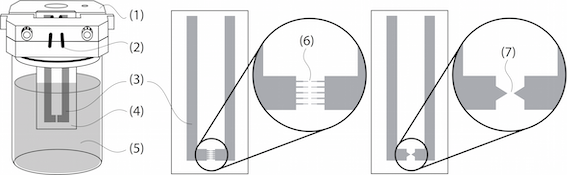
Figure: Electrochemical cell for nanoscale electrocrystallization
In the electrocrystallization (not nanoscale), electrolysis is performed under direct current (DC) condition. In the nanoscale electrocrystallization, of course it is possible to perform electrolysis with DC and grow crystals only on one electrode. In addition to this, the nanoscale electrocrystallization enables us to form nanocrystal bridging structures that are advantageous for electronic property measurement and device applications only using alternating current (AC) electrolysis.
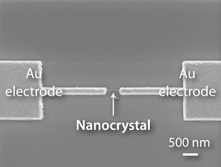
Figure: Nanocrystal growth using nanoscale electrocrystallization
This technology is marketed as a “Nanowire Fabrication Kit” and we are working to popularize the technology so that it can be easily tested in the laboratory.
Device fabrication using the nanoscale electrocrystallization
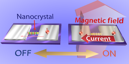
Such nanocrystals are bridging between two electrodes not only visually but also electrically. When external electric or magnetic field are applied to the nanocrystals, their electrical characteristics will change. We are utilizing these phenomena to make devices and evaluating them.
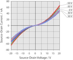
Field-effect transistors (FETs), which are also used in personal computer CPUs, are known as devices whose characteristics change due to change of external electric field. When the characteristics were measured by applying voltage from a third electrode to a nanocrystal produced by the nanoscale electrocrystallization, a change in electrical current was confirmed although it was weak. The characteristics are not enough to utilize a transistor, so we are looking for a more suitable material and preparing nanocrystals to measure their characteristics.
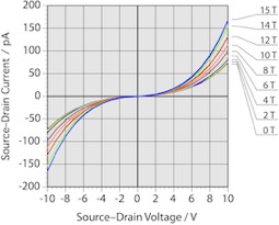
On the other hand, there are materials whose characteristics change by external magnetic field. The magnetic head of a hard disk uses this phenomenon. In this study, we created a bridging structure by nanoscale electrocrystallization using dicyanoiron (III) phthalocyanine, which is known to show negative magnetoresistance effect in bulk (visible size) crystals, as a starting material. When a magnetic field was applied to this nanocrystal, increase of the current due to the negative magnetoresistance effect was observed at the nanoscale as well as bulk state. By minimization of the crystal, the entire substrate can be utilized as a device as it is.
In another material, switching characteristics were seen that changed (switched) from low conductive state to high conductive state when a voltage was applied. Attempts are being made to control this property.
These characteristics still need to be improved in order to be used as a practical device. In addition, the use of novel materials will uncover unknown characteristics and may result in unprecedented devices. Currently, we are aiming to improve performance by devising materials and structures. Additionally, we are also trying to fabricate nanocrystals via a vacuum-free process using an inkjet printer. Through this research theme, we aim to realize 21st century nanofabrication that is both economically and environmentally friendly in the future.
Functional Manifestation by Inkjet Patterning of Biomaterials and Its Application
Biomimetics
In recent years, the construction of new biomimetic artificial systems that take advantage of the advanced functions of biological systems has attracted attention. Biomimetics is a concept that can be used in the real world by imitating shapes, structures, and functions of natural things. For example, in the familiar area, a number of biomimetics are used in the Shinkansen 500 series. The top shape mimics the kingfisher's beak to prevent tunnel micro-pressure waves. Also, in order to prevent wind noise from pantographs, a material that mimics the shape of the owl's wings is used (not used at the time of “Kodama”). In addition, the body has a light-weight and high-strength honeycomb structure. In this way, biomimetics "learning from nature" is used in various places.
In this research, we are aiming to develop a “visual sensor” that mimics the “visual function” of living things. Another feature of this sensor is that it uses the bacteriorhodopsin (bR), a photoreceptive membrane protein extracted from the cell membrane of highly halophilic bacteria, which is a biological material.
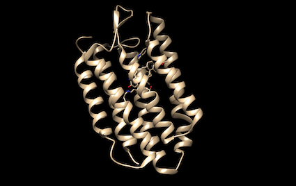
Figure: Molecular structure of bacteriorhodopsin
Bacteriorhodopsin and visual sensors
However, there is a big problem when fabricating a device like a sensor with biomaterials. Because biomaterials are generally vulnerable to heat, chemicals, and drying, for example, they are not suitable for semiconductor manufacturing processes. Since it is necessary to create various shapes for the production of a visual sensor, a technology for freely patterning under mild conditions suitable for biomaterials was required. Therefore, this research aims to develop a technique for freely patterning bR under mild conditions by the inkjet method.
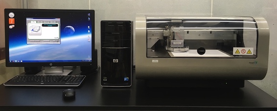
Figure: Material printer Fujifilm Dimatix DMP-2831
Also, as sensors that mimic visual functions, we are making “DOG filters” and “Gabor filters” that are also included in the vision of living bodies. The “DOG filter” has a function to recognize the contour of an object, and the “Gabor filter” has a function to recognize the movement and direction of an object.
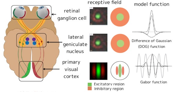
Figure: Structure of visual receptive field (Illust. by Prof. Okada-Shudo (UEC))
Patterning and functional manifestation
Using biomaterials does not mean that a visual sensor can be made. Here, we are only using the function of bR, a biomaterial, that absorbs light and releases hydrogen ions (H+). In order to make good use of this function and bring out the image recognition function, figures (patterns) are created using bR. The sensor that imitates the visual function can be realized for the first time by designing the pattern in consideration of the light response characteristics of bR. The inkjet method is used to create this pattern.
Function and Physical Properties of Organic-inorganic Hybrid Perovskite Compounds
Organic-inorganic hybrid perovskite compounds
In developing high-performance electronic devices, it is important to control the electronic structure of the material. For example, in solar cells, efficiency can be increased by creating an energy difference that matches the wavelength of the light that is absorbed. Transistors also enable efficient carrier injection by combining the Fermi level of the metal electrode and the energy level of the band of the channel material. Such electronic structure control has been realized by high-energy processes such as ion implantation, which has been found in the semiconductor industry. On the other hand, considering the environmental impact, it is expected that the electronic structure of materials will be controlled in the future by a method with lower energy consumption, such as solution process.
Perovskite compounds are known as compounds whose electronic structure can be easily controlled by substitution of constituent elements such as superconductors and dielectrics. Among them, organic-inorganic hybrid metal halide perovskites are generally soluble in organic solvents, etc. in addition to excellent electronic properties such as high mobility, and have advantageous features in applications such as device fabrication by solution process. It is. In fact, it has been reported as a high-performance field-effect transistor. Recently, it has been actively researched as a promising solar cell material, and has attracted attention as a next-generation electronic material.
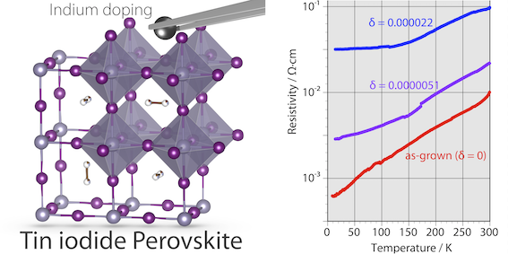
Generally, metal halide perovskite is an insulator that does not conduct electricity, but it has long been known that tin iodide organic / inorganic hybrid perovskite compounds exhibit high conductivity. In our previous research, we investigated the origin of the high conductivity. Although this material is a semiconductor with a band gap of 1.3 eV, it was found that the temperature dependence of electrical conductivity and the temperature dependence of thermoelectric power show metallic behavior. When the doping level was examined from Hall effect measurement, it was found to be 0.02%. Consequently, it was concluded that this material was a doped semiconductor.
In this study, we are investigating the effects on the electronic structure and properties of metal halide organic-inorganic hybrid perovskite compounds that can be prepared in solution by substituting some of the constituent elements with other elements. We have already reported the effects of substitution to bromine, bismuth or indium in methylammonium tin iodide cubic perovskite. Through this research, we aim to establish effective guidelines for the design of electronic materials.
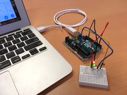
Development of Programming Materials Suitable for Science Classes
Science and programming education
From 2020, programming education was introduced in elementary schools. This education is not aimed at learning programming itself, but the most convenient way to develop computational thinking is to acquire the ability to create programs actually. However, it is difficult to take additional programming time in addition to regular classes, and to prepare specialized teachers. Therefore, we are developing teaching materials to provide an environment in which programming can be practiced in the classes of ordinary subjects. Specifically, in science classes, children think of programs that automatically read environmental data such as temperature and brightness, and cause some movement based on it, and learn programming skills through it. In fact, even in our advanced research, we often build our own programs to measure physical property data. Therefore, we are studying a comprehensive programming learning environment in collaboration with science and developing teaching materials that match it.